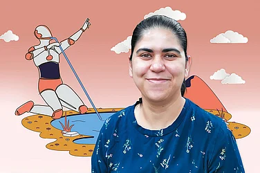


India's semiconductor policy is moving towards a broader ecosystem covering design, manufacturing and talent
Packaging, OSAT, memory and certain raw materials remain major bottlenecks, said Mindgrove Technologies CEO Shashwath TR
He added that policy stability is more important than a drastic policy change
India’s semiconductor push is moving beyond fabs to build a wider ecosystem spanning chip design, intellectual property, advanced packaging, R&D, materials and talent. But for Indian fabless companies, designing a chip is only the first step. Moving it from tape-out to manufacturing, packaging, testing, qualification and, eventually, customer adoption can take years.
Mindgrove Technologies is now entering this commercialisation phase as it prepares to take its chips to market. In an interview with Outlook Business, Co-founder and CEO Shashwath TR said packaging and testing remain major challenges for fabless companies.

1 September 2026
Get the latest issue of Outlook Business

He further stressed the need for more Indian product companies that own and commercialise their intellectual property. The company is also seeking additional funding as it evaluates the support available under Semicon 2.0.
Below are the edited excerpts of the interview:
Semicon 2.0 has expanded the focus beyond fabs to design, IP, talent and manufacturing. Where is India's semiconductor ecosystem headed, and what needs to change?
I think the change is already happening and the evidence of the change is India Semiconductor Mission (ISM) 2.0, and indeed the ISM 1.0. What we really need is for the policy to remain consistent and make logical changes as our experience tells us what works and what doesn't, which is basically what ISM 2.0 is.
ISM 1.0 was kind of piecemeal. They had an ISM which was focused on manufacturing and then they had a DLI (Design Linked Incentive Scheme) which was focused on design. Now, instead what they have done is built all these six pillars and then said that design, manufacturing, talent development, skill development, all of these are just pillars of ISM. So, that allows them to pull a lot of things together.
But traditionally, India was always the place where the development happened and not the product ideation. And that needs to change and we need to own our own products. That's probably the hardest part of it, sociologically, not technically. To take the risk and say I'm going to build a product because I see a market opportunity.
Advertisement
What are the biggest bottlenecks in India's semiconductor ecosystem right now?
Packaging is a huge bottleneck. Outsourced Semiconductor Assembly and Test (OSAT) is a huge bottleneck. We're making some improvements over there, but unlocking that will actually lead to a lot more comfort in the ecosystem.
The memory is a bottleneck, largely because of AI and what is going on in the industry. Certain raw materials, chemicals, and stuff are bottlenecks because of the war.
For semiconductors, per se, critical minerals don't matter too much, because most of what we do is silicon, and on top of silicon, it's copper. What really matters is the chemicals which are used in processing and building this thing (semiconductor chips). It's all chemical engineering mainly.
Advertisement
What will determine whether India's semiconductor design companies become sustainable product businesses rather than remaining primarily design-service or engineering companies?
A lot of product thought and a lot of product development. Now, that has traditionally been our weakest link.
About 20% of all semiconductor engineers are resident in India. And not a chip goes out that is not touched by an Indian, sitting in India.
But traditionally, India was always the place where the development happened and not the product ideation. And that needs to change and we need to own our own products.
We've been on the services treadmill for long enough. A good significant percentage of those 20% of engineers, the semiconductor engineers, are actually sitting in IT services companies, doing semiconductor design as an IT service for some of the global majors.
What is Mindgrove building, and why did you choose the system-on-chip route?
The more basic thing that we are is a fabless semiconductor entity. Fabless means we do not own our own foundry and we contract out the manufacturing to other companies such as TSMC or eventually the Tata foundry (which is currently being built).
What we build as a fabless semiconductor company can be anything from RF chips, analogue chips, small devices which power management, and all the way to processes that work in data centres and clusters.
What we do is we are largely in the few million transistor level. We build things which are largely tailored towards computer vision, signal processing and security, and microprocessors and microcontrollers.
A system-on-chip is a term of art. When I say we do stuff for signal processing and computer vision security, those security accelerators, those vision accelerators, the signal processing accelerators get designed into a single chip, which has its own tiny network on the chip to connect all of these components together.


What are the biggest challenges in taking an Indian-designed chip from architecture and tape-out towards actual customer adoption and commercial revenue?
The design for a small chip can take at least six to eight months. For a large chip, it could be even two years. Then it takes three months or upwards of three months to manufacture the chip and give it back to me.
And packaging takes another few weeks, months, sometimes as much as a year. Because Assembly, Testing, Marking, and Packaging (ATMP), OSAT can have a huge backlog for the companies in the industry. There's not much work, but then the foundries and manufacturing firms are backed up to the line. You have to wait for a slot on the line.
So, if I'm making a bet this year about a chip which is going to come out next year or the year after. So, the time period is a big challenge.
For a small microcontroller, it could take a year or two. For a very complex chip, it could take as much as five or six years.
Hence, the biggest lesson is probably the packaging. It is always the packaging and the testing. The packaging can have thermal problems, electrical problems. The foundry is the easy part. Packaging and testing is the hardest of the lot.
You have said Mindgrove expects to generate revenue this year. What are the challenges for the company as it moves towards commercialisation? How many chips has the company produced?
Actually, zero [chips in the market]. In 2024, our prototype came out. And right now, we are at the cusp of launching that prototype which became a production chip into the market. And that's going to take another one or two months for us to actually finish all the issues and get it out into the market.
So, that's just how long it takes. It's not like there were no mistakes along the way. We had to make some changes. We had to fix the design, go back and forth. But it takes that long to take a chip from concept.
I said I want to have revenue this year, so it's this year. By the end of the 2026 calendar year. We're fine-tuning a lot of things at the last minute. We are getting it into the market, and we have to make sure that everything is perfect before we get it in.
It's not just about that, it's about distribution, it's about stock, and all those kinds of things. We're just working out all those things before. I want our customers to have an experience where they can order chips, and we tell them, okay, we will get your chips by this time, and this is what it will cost you. And then they have chips on the date that they were told, and they will be able to use them. I don't want any faults in that, so we're just taking our time to make sure that that happens perfectly.
As a semiconductor startup, are you looking for more funding?
As I've told people before, we are a fabless semiconductor startup. Of course, we're looking for funding. So we will be looking for money. We are always looking for money.
I'm not going to announce a round or anything right now. We're thinking about what to do. We were waiting for the semiconductor ISM 2.0 to come out so that we could figure out exactly where we will get government support and where we will need money to invest.
What is still missing for India to produce a globally successful semiconductor product company?
I don't know if there is a gap yet. I can't tell you that this is the gap, because I can't analyse a gap without having seen a couple of real-world attempts at deployment and see how they fail or not fail.
We can't predict what is going to happen, as something that you think is sorted might actually be a huge problem, and something that you think is easy might be a huge problem.
That we'll only know in the coming days as us and our peers take our chips to the market, drop them into the market and see what happens.