
India targets 3-nm chips by 2032 and 2-nm by 2035 to rank among the top four semiconductor nations
By 2029, India aims to meet 70–75% of chip demand domestically and handle nearly 50% of global chip design
Semicon 2.0 will support 50+ fabless start-ups, expand DLI, and launch Deep Tech Awards
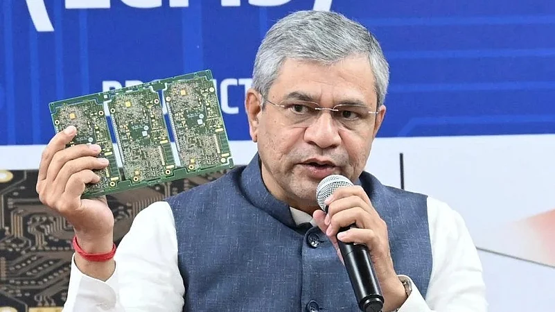
Building on a strong chip design ecosystem, India is now aiming to reach the capability to manufacture 2-nanometre semiconductor chip by 2035, said Union Minister for Electronics and Information Technology Ashwini Vaishnaw on Tuesday.
He was addressing the executives of 23 chip design companies approved under the Design Linked Incentive (DLI) Scheme of the Semicon India Programme.

1 June 2026
Get the latest issue of Outlook Business

“From here, we move to the next level. By 2032, we aim to achieve 3-nanometer manufacturing capability. We have studied how South Korea, Taiwan, and Japan achieved this, and we have developed a well-thought-out strategy that will be part of Semicon 2.0,” he said.
He also mentioned that by 2035, India should be among the top four semiconductor nations in the world.
Vaishnaw also announced that the ministry will organise the Deep Tech Awards in November–December to recognise start-ups and companies across sectors such as semiconductors, artificial intelligence, biotechnology, and space that are pushing technological boundaries and creating new frontiers.

Emphasising the growing strength of India’s domestic chip design ecosystem and ownership of intellectual property, the Union Minister said the government aims to ensure that by 2029, India will have the capability to design and manufacture semiconductor chips required for 70–75% of domestic applications.
“I can say with high confidence that in the coming years, nearly 50% of the world’s semiconductor design work will be done in India. And the most exciting change is this: many of our brightest minds, who earlier worked for others, will now build companies of their own. They will create jobs, generate patents, develop IPs, and strengthen the nation,” Vaishnaw added.
For semiconductor design start-ups and companies, Vaishnaw outlined six major system categories to comprehensively develop India’s semiconductor design ecosystem.


These include compute and logic, including high-performance computing and microcontrollers; RF technologies, covering millimetre-wave and all relevant frequency bands; networking, with a special emphasis on secure and cyber-secure systems; power management; sensors, which enable the conversion of the physical world into the digital domain; and memory, which completes the semiconductor system stack.
“Any major system whether drones, missiles, defense equipment, automobiles, railways, space systems, or industrial applications uses a combination of these six building blocks. Once we master them, we can do nearly 80% of the work domestically,” he said.
Concluding his address, the Union Minister for Electronics and IT said that the ministry plans to significantly scale up support under the next phase of the Semiconductor Mission, with a target of backing at least 50 fabless semiconductor companies in the country.