India set to train over 100,000 engineers through SMART-S, SEMI-verse & other schemes
Around 550 institutions roll out new semiconductor-focused programs this year
India now ranks in global top 10 for semiconductor-related research publications
India has logged more than 10 million student hours on electronic design automation (EDA) tools this year, the largest such youth access programme in the world, a senior education official said on Wednesday.
“This alignment of education with industry requirements is one of the most significant reforms shaping India’s semiconductor future. The results are already visible: more than 280 institutes and 70 student clubs are supported with Electronic Design Automation (EDA) tools. India today runs the world’s largest EDA tool support program, logging over 10 million student usage hours this year alone,” Vineet Joshi, Secretary, Department of Higher Education, Ministry of Education, said.

1 June 2026
Get the latest issue of Outlook Business

EDA tools are specialized software applications used to design, simulate, and test electronic systems such as semiconductors, integrated circuits (ICs), and printed circuit boards (PCBs).
DHE Secretary highlighted that semiconductor innovation from our Indian institutions has become a vehicle for sustained growth.

According to him, With a median age of just 28.8 years, India has the world’s youngest workforce.
“By 2026, India will produce 5,000 highly skilled professionals in semiconductors, close to 10 million students in the STEM pipeline, more than 3,100 universities, and 52,000 colleges,” he added.
Joshi also informed that academic fabs are also performing at par with global peers, contributing not only to training but also to innovation.
He also cited examples of pressure sensors developed at IISc Bengaluru that are being used in space missions, apart from nanotechnology-based explosive detectors developed at IIT Bombay that are deployed at high-security sites.
Highlighting the skill gap in India’s semiconductor industry as a key concern, Joshi said that over 550 institutions have introduced semiconductor-focused programs from this academic year and in the next few years, thousands of engineers trained in this field will be available to the industry.
He appreciated the programs like Chips-to-Startup and the Design-Linked Incentive (DLI) scheme under MeitY that are preparing 85,000 design engineers.
“At IISc, the SEMI-verse virtual platform is training 60,000 students in advanced design. Through the Skill Development for Advanced Research and Training in Semiconductors (SMART-S) program, we aim to skill over 100,000 engineers in semiconductor technologies,” Joshi noted.
According to the Secretary, DHE, this industry-academia–research synergy has enabled India to rank among the world’s top 10 countries for research publications in this field.
Highlighting the challenge, he noted that to compete with established talent powerhouses such as China, Korea, Taiwan, and the United States, the India Semiconductor Mission (ISM) roadmap envisions the need for around 5,000 globally recognized researchers.
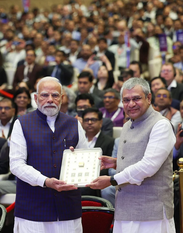
Joshi was speaking on the 2nd day of Semicon India 2025 about the semiconductor industry and how the education sector is addressing its workforce and skill development needs.