


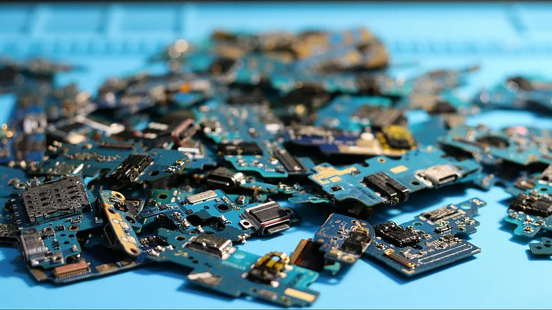

Uttar Pradesh has granted conditional clearance to two semiconductor proposals and is awaiting final approval from the Union IT Ministry
Under its current 2024 policy, Uttar Pradesh offers a 50% top-up on the Centre's fiscal support alongside land and power subsidies
The state government plans to continue supplementing central incentives to attract major semiconductor fabrication and packaging units
Uttar Pradesh has conditionally approved two semiconductor proposals filed during the debut phase of the India Semiconductor Mission (ISM), as per a report by Moneycontrol.
The state is now waiting for the Union IT ministry to sanction the plans.

1 September 2026
Get the latest issue of Outlook Business

Himanshu Kaushik, Managing Director of the Uttar Pradesh Electronics Corporation Limited (UPECL), said the state has already granted conditional clearances and is awaiting the Centre's approval.



"There are two proposals with the Government of India. We have already given conditional approval from our side and are awaiting the Centre's approval," Kaushik said, as per Moneycontrol.
The exact nature of the projects remains unclear. Kaushik declined to clarify if the applications involve chip fabrication plants or packaging facilities, saying he needed to verify the details first.

Preparing For Semicon 2.0
The Union Cabinet approved Semicon 2.0 earlier this month, and the Ministry of Electronics and Information Technology (MeitY) is preparing to roll out detailed guidelines.
Advertisement
Uttar Pradesh, which unveiled its semiconductor policy in 2024, is also preparing to review its incentive framework once the new guidelines are notified.
"We are waiting for the guidelines from the Government of India. Once we receive them, we will analyse Semicon 2.0 and, if required, come up with an amendment or a new semiconductor policy," Kaushik said, as per the report.
State Incentive Framework
The current state policy offers deep discounts as Uttar Pradesh matches half of the financial aid granted by the Centre and slashes land acquisition costs by 75%.
Firms also secure a decade-long waiver on electricity duty alongside stamp duty concessions.
Advertisement

Silicon fabrication subsidies remain capped at 40% of setup costs. But the Union Cabinet lowered financial aid for certain packaging ventures.
The state wants to keep matching federal subsidies. "We will continue to do so, but we will study the new framework before deciding whether any substantial changes are needed," Kaushik said.
What Centre Plans Under Semicon 2.0
Semicon 2.0 marks the next phase of India's semiconductor mission, with a broader strategy centred on six key focus areas: chip design, semiconductor equipment and materials, fabrication facilities, packaging and assembly, research and development, and talent development.
The initiative seeks to promote indigenous semiconductor intellectual property (IP), support chip and system-level product design, and draw fresh investments into silicon fabrication plants, compound semiconductor and display manufacturing facilities, as well as advanced packaging units.
According to the government, the expanded programme is designed to reinforce India's presence across the entire semiconductor value chain, enhance supply chain resilience, and strengthen the country's technological capabilities.
The first phase of the India Semiconductor Mission (ISM), launched in 2021 with a financial outlay of ₹76,000 crore, focused largely on creating a domestic semiconductor manufacturing ecosystem through incentive-based support.
Semicon 2.0 widens the mission's scope by extending support to semiconductor manufacturing equipment, speciality chemicals, industrial gases, research infrastructure, and chip design capabilities.