
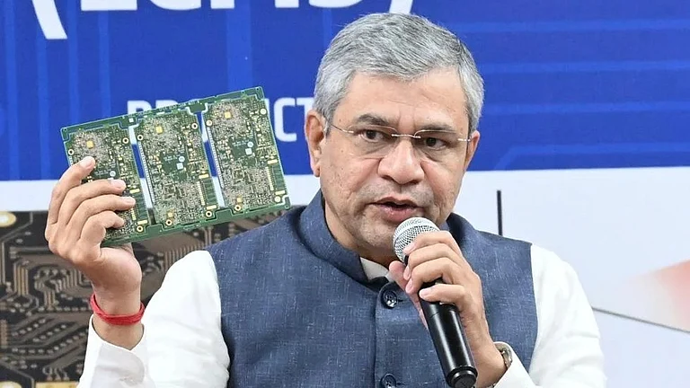
Union Minister Ashwini Vaishnaw on Sunday said the Centre's Semicon Mission 2.0 will focus on bolstering deep tech startups, prioritising the creation of a design ecosystem and getting equipment manufacturing and design facilities in the country.
Addressing the inaugural session of the Gujarat Semiconnect Conference 2026 here, the Union Minister for Electronics & Information Technology said that a talent gap of 20 lakh in the semiconductor sector will create huge opportunities for students.
"Semicon 2.0 will be totally the reverse of Semicon 1.0, which focused on getting manufacturing facilities in India. We got that. We have 10 plants, with the first starting commercial production yesterday. Very soon, the second plant will start commercial production," he said.

3 February 2026
Get the latest issue of Outlook Business

Vaishnaw said that the top priority for Semicon 2.0 — the second phase of India's Semiconductor Mission — will be to create a "design ecosystem", so that deep tech startups get the opportunity to develop the next Qualcomm, Broadcom, or Nvidia.
"And it is not going to be an easy journey; it's going to be a humongous task, and we understand the complexity of it. That's why, we are very realistic and pragmatic about it," he said.
The deep tech startups ecosystem will focus on semiconductor design and creating innovative products, which can then be manufactured in the fabs, he said, adding that the next priority will be getting the equipment manufacturing and design ecosystem in the country.
Vaishnaw pointed out that it is vital to have a material, machine, equipment, testing and validation ecosystem well established in the country for the foundation of the 20-year journey to be very strong.
He stated that talent, which has been a very big priority in Semicon 1.0, will remain a priority in Semicon 2.0.
"In the first version, we promised 85,000 engineers would be trained in semiconductor design in 10 years. It has been achieved in 4 years itself," he said.


The Union minister further noted that as the semiconductor sector globally grows from $800-900 billion to a trillion-dollar industry, a 20 lakh talent gap that the second phase creates will mean opportunities for students.
"We are prepared for that. From 350 (in Semicon 1.0), we will take it to 500 universities. Every state will have so many universities and colleges where students can get trained in semiconductor design, manufacturing, testing and validation — and that will create a huge, continuous stream of opportunities in youth," he said.