As India moves ahead in its semiconductor ambitions, Tata Electronics is prioritizing workforce development to build a skilled talent pool. The company has assembled a leadership team with over 2,000 cumulative years of experience and is collaborating with IITs and IISc Bangalore to train future chip engineers.
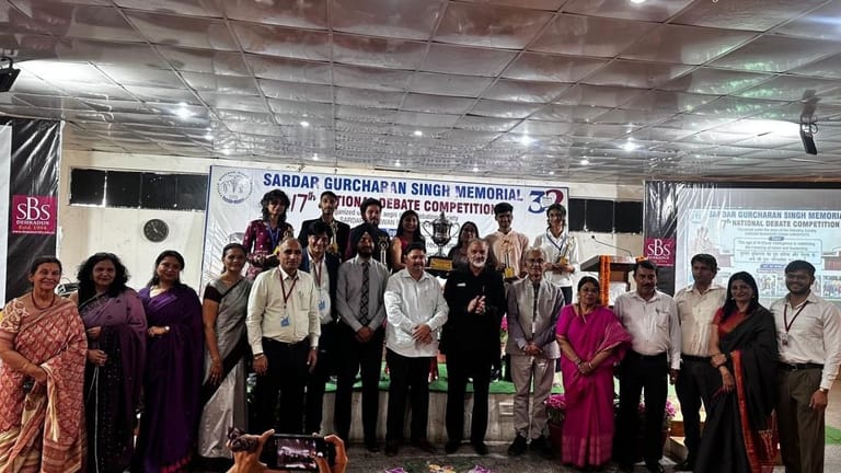
Speaking at an event, SVP of Tata Electronics, Utpal Shah, outlined the company’s ambitious plans in India’s semiconductor industry.
He highlighted the establishment of India’s first commercial 12-inch semiconductor fab in Gujarat’s Dholera and the company’s focus on nanoelectronics, technology, and talent development.
Shah stressed that India’s cost competitiveness and environmental sustainability would be key advantages in the global semiconductor market over the next decade. “We are starting our fab with 100% green power and nearly 100% water recycling,” he said, emphasising that such initiatives would position India as a leader in environmentally conscious manufacturing.
Tata Electronics, launched in May 2020, is currently operating manufacturing sites, with 65,000 employees across 1,800 acres. The Dholera fab, set to produce up to 50,000 wafers per month, aims to cater to India’s growing demand.
The facility will use technology from Taiwan’s PSMC, with whom Tata Electronics closed a partnership last September.
“We are replicating their fab design to accelerate our schedule,” Shah explained, adding that the project enjoys strong government backing 50% funding from the central government, 20% from Gujarat, and 30% equity from Tata.
On the talent front, he pointed to investments in skilling India’s workforce. “We have built a leadership team with over 2,000 cumulative years of experience,” he said, noting collaborations with IITs in Gandhinagar, Guwahati, and Bombay, as well as IISc Bangalore. “For India’s semiconductor dream, we need a sustained supply of skilled professionals, from fresh graduates to senior experts.”
Beyond the fab, Tata Electronics is making strides in packaging technology. The company’s facility in Bangalore, operational since December 2023, has developed technologies such as Wire Bond, Flipchip, and ISP. “We are among the first Indian companies to package chips domestically, including India’s first indigenous Shakti microprocessor from IIT Madras,” Shah stated.
A large-scale OSAT facility in Assam, with a $3 billion investment, is slated for high-volume manufacturing by 2026.
Shah stressed the need for deeper industry collaboration, increased venture capital funding, and policy support to accelerate India’s semiconductor ambitions. “This is nothing like what India has done before,” he said.


